尚丰科技向用户提供专业的的电子束吸收电流分析系统EBAC/RCI
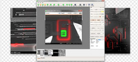
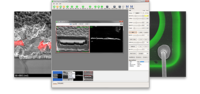
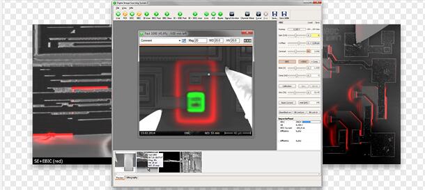
EBAC-RCI原理EBAC/RCI电子束吸收电流分析系统,能够方便快速的定位半导体芯片电路中的短路及失效点位置,不但可以对同层电路,而且可以对次表层,甚至表层下第三层、第四层电路进行失效点的定位,因此能够对半导体芯片电路或相关材料进行快速准确的失效分析。
目前,集成电路芯片设计越来越复杂,关键尺寸和金属连线线宽越来越小,传统的失效点定位方法,如微光显微镜或光束又到电阻变化鞥,由于其分辨率不足,导致不能精确地定位电路故障点位置,电压衬度方法虽然在一些开路短路失效分析中能快速地定位失效点,但只是局限于电路同层分析。
EBAC/RCI电子束吸收电流分析系统是基于扫描电镜的分析系统,在保留扫描电镜高分辨率的前提下,能够对同层芯片电路进行高定位,同时能够对次表层甚至表面下第三、第四层电路进行失效点定位,因此越来越多的应用于先进制程芯片的失效分析。在涉及多层金属层的失效定位分析时,EBAC/RCI方法更加简便精确,可保证分析的成功率,并缩短分析周期。
EBAC/RCI acquisitionThe lowest noise Electron Beam Absorbed Current (EBAC)and Resistive Contrast Imaging (RCI)
Find exact location of any open,resistive or shorting defect
Localize metal line cuts caused by cracking,corrosion, electro-migration, or foreign particles
Identify resistive opens caused by interface contamination at via interconnects
Pinpoint location for direct TEM lamella FIB preparation
Characterize interconnects with highest resolution
Reveal electrical integrity of nets with sub-mciron lateral resolution and bridge from EFA to PFA
Diagnose fabrication and long term issues, including contamination,metal pattering defects, resistive interconnectors, or electro-migration
Directly isolate defects to the exact layer and die location, and improve them to product improvement actions
Verify device operation modes with built-in biasing for voltage contrast
Image bias/voltage contrast in delayered devices
Monitor operation of devices under bias
Compare imaged behaviour with device design
Localize defects in thin dielectric layers
Visualise and localise weaknesses in gate oxide (GOX) and capacitor oxide (COX) before breakdown
Pinpoint oxides shorts caused by ESD or EOS with sub-micron resolution
Preserve the original defect signature with power dissipation in the lower nW range during localization
Access failures invisible in voltage contrast
Find low resistances that allow charge tunneling trough the interconnects
Investigate structures in contact with the silicon substrate
Characterize large metal structures
尚丰科技致力于引进推广先进的材料、生物显微观测及微区分析仪器,向科研人员提供高附加值服务。我们拥有一支涉及众多领域高素质的应用支持团队,为各行业的应用需求提供专业的解决方案和售后服务。
敬请联络
尚丰科技(香港)有限公司