尚丰科技向用户提供专业的的电子束感生电流分析系统EBIC
EBIC原理
当扫描电镜电子束作用于半导体器件时,如果电子束穿透半导体表面,电子束电子与器件材料晶格作用将产生电子与空穴。这些电子和空穴将能较为自由地运动,但如果该位置没有电场作用,它们将很快复合湮灭(发射阴极荧光),若该位置有电场作用(如晶体管或集成电路中的pn结),这些电子与空穴在电场作用下将相互分离。故一旦在pn结的耗尽层或其附近位置产生电子空穴对,空穴将向p型侧移动,电子将向n型侧移动,这样将有一灵敏放大器可检测到的电流通过结区。该电流即为电子束感生电流(EBIC)。由于pn结的耗尽层有很多的多余载流子,故在电场作用下的电子空穴分离会产生很高的电流值,而在其它的地方电流大小将受到扩散长度和扩散寿命的限制,故利用EBIC进行成像可以用来进行集成电路中pn结的定位和损伤研究。
EBIC应用领域包括但不限于:
1)材料晶格缺陷探测分析,缺陷以黑点和黑线标识出来;
2)P-N结缺陷区域定位;
3)双极电路中导致集电极-发射极漏电电流的收集管路的探测;
4)探测额外连接或者多层掺杂;
5)确定静电放电/电过载(ESD/EOS)导致的失效位置;
6)测量减压层/耗尽层(depletion layer)宽度和少数载流子扩散长度和时间(minority carrier diffusion lengths/lifetimes)
等等。
EBIC图像对于电子-空穴的重新组合非常敏感,因此EBIC技术能够非常有效的对半导体材料缺陷等进行失效分析。
BenifitsMake the link between device characterization and materials properties
Image electrical activity across complete devices
Distinguish between electrically active and passive defects
Correlate electrical activity with composition (EDS) and crystallographic structure (EBSD)
Localise electrical defects with highest resolution
Enable sample preparation for TEM or atom probe microscopy
Avoid alignment errors by directly imaging defects with EBIC in FIB SEM
Use live EBIC imaging to stop milling during sample preparation
Map junctions and defects over large areas
Identify all electrically active defects
Map active areas of junctions and electrical fields
Validate doping profiles and areas
Export calibrated EBIC signal for analysis of materials properties
Measure defect contrast / recombination strength
Extract diffusion length of minority charge carriers
Determine width of depletion regions
Verify device operation modes with built-in biasing and live overlay
Image junctions and fields in delayered devices
Map electrical activity in solar cells under bias
Compare imaged behaviour with device modelling
Access third dimension with depth profiling
Manipulate depth of EBIC signal by changing kV in SEM
Investigate EBIC images of cross-sections in FIB-SEM
Export EBIC depth series for 3D reconstruction
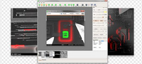
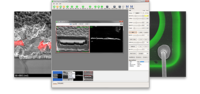
FeaturesThe EBIC system is fully integrated and software controlled
Image acquisition and EBIC module are integrated into one software
All amplification and acquisition settings are software controlled
EBIC signal is automatically quantified and displayed in current values (μA, nA, pA)
The most sophisticated and easy to use EBIC amplifier
Two stage amplification for maximum gain range
Built in -10…+10V DC bias with current compensation
Beam current output for SEM feedback and integration
The most powerful and versatile SEM scanning system – DISS5
Integrated scan generator and image acquisition
Very large image resolution, up to 16k x 16k pixels
Very fast scanning speed, down to 200ns dwell time
Simultaneous 4x analogue and 12x digital counter inputs
Optional electrical sample holder for large area devices
Suitable for solar cells, photovoltaics and light emitting diodes
Flexible mount in plan-view or cross-section configuration
Includes Faraday cups for beam current measurements
Advanced controls are provided for calibration, biasing and scanning
Flexible pre-amplifier gain from as little as 10^3 to as high as 10^10 V/A
Further 0.1…100x gain and 100 μA compensation for optimum imaging
Electronics are optimised for high speed, providing 0.5 MHz at 10^9 V/A
Simultaneous signals are mixed live for correlative microscopy
Up to 4x simultaneous signals
12-bit digitization with signal integration (oversampling)
Live colour mixing tool for visualisation
Current-voltage (IV) tool is integrated for contacts and nanoprobing
Voltage output maximum range is -10…+10 V
Gain selection for current measurements is automatic
IV may also be used for device characterisation
Configurable scan profiles enable custom workflows for efficient use
Fast EBIC scan profile for alignment and navigation
High resolution EBIC scan profile for mapping and analysis
Simultaneous SE/EBIC scan profile for localization
Live signal monitor assists image acquisition and calibration
Live line scan signals are displayed for optimisation
Multiple live signals are displayed simultaneously
The gradation graph improves display of complex shadows
Advanced live scan tool enables advanced beam control
Select points, lines or areas from pre-scan images
Set number of points, step size, binning and averaging
Generate single or multiple diagrams
Export diagrams and/or raw data
Gallery
尚丰科技致力于引进推广先进的材料、生物显微观测及微区分析仪器,向科研人员高附加值服务。我们拥有一支涉及众多领域高素质的应用支持团队,为各行业的应用需求提供专业的解决方案和售后服务。
敬请联络
尚丰科技(香港)有限公司